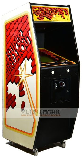
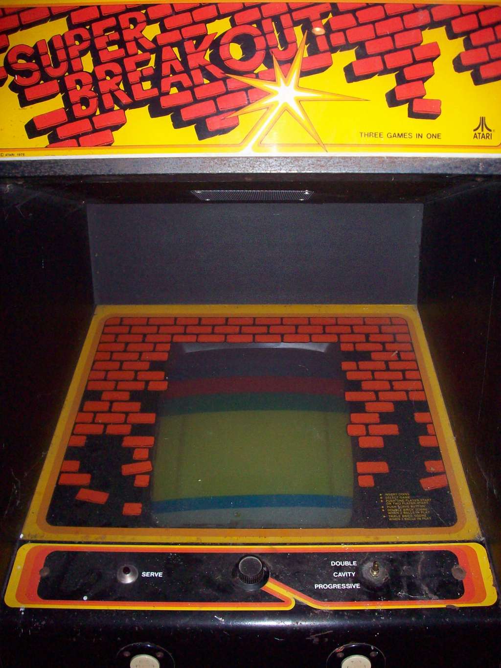
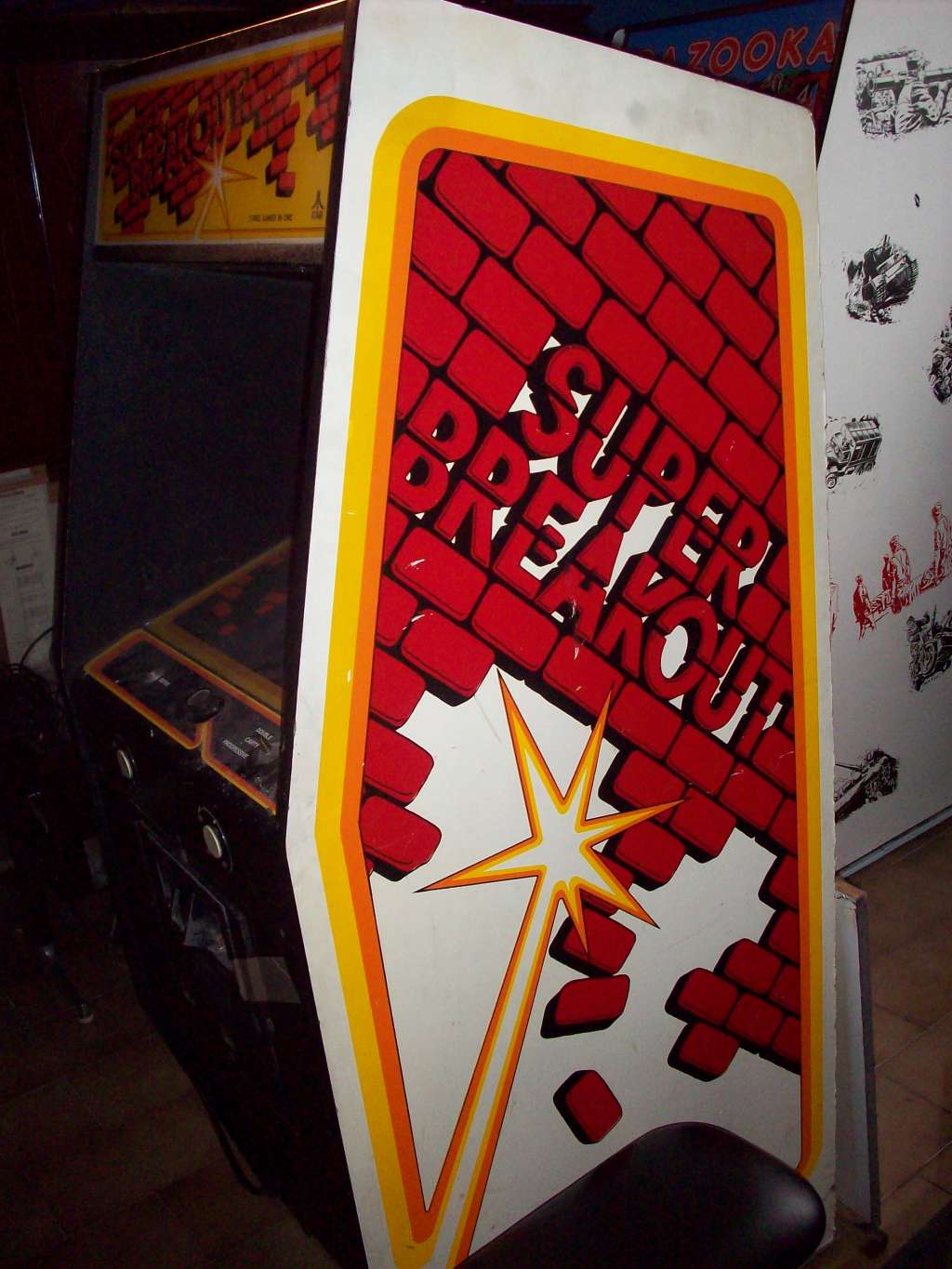
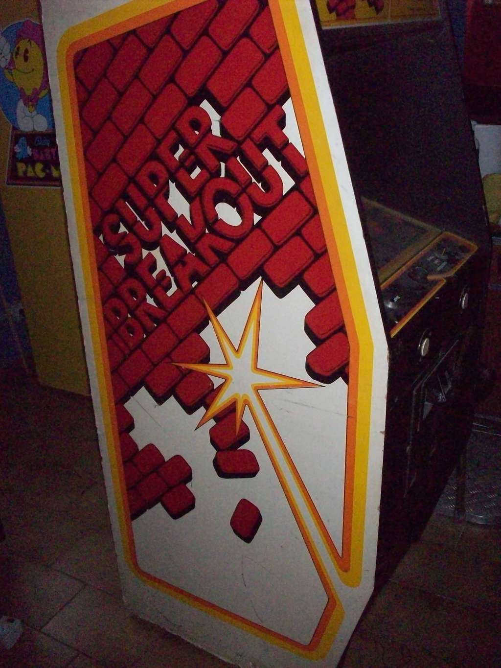
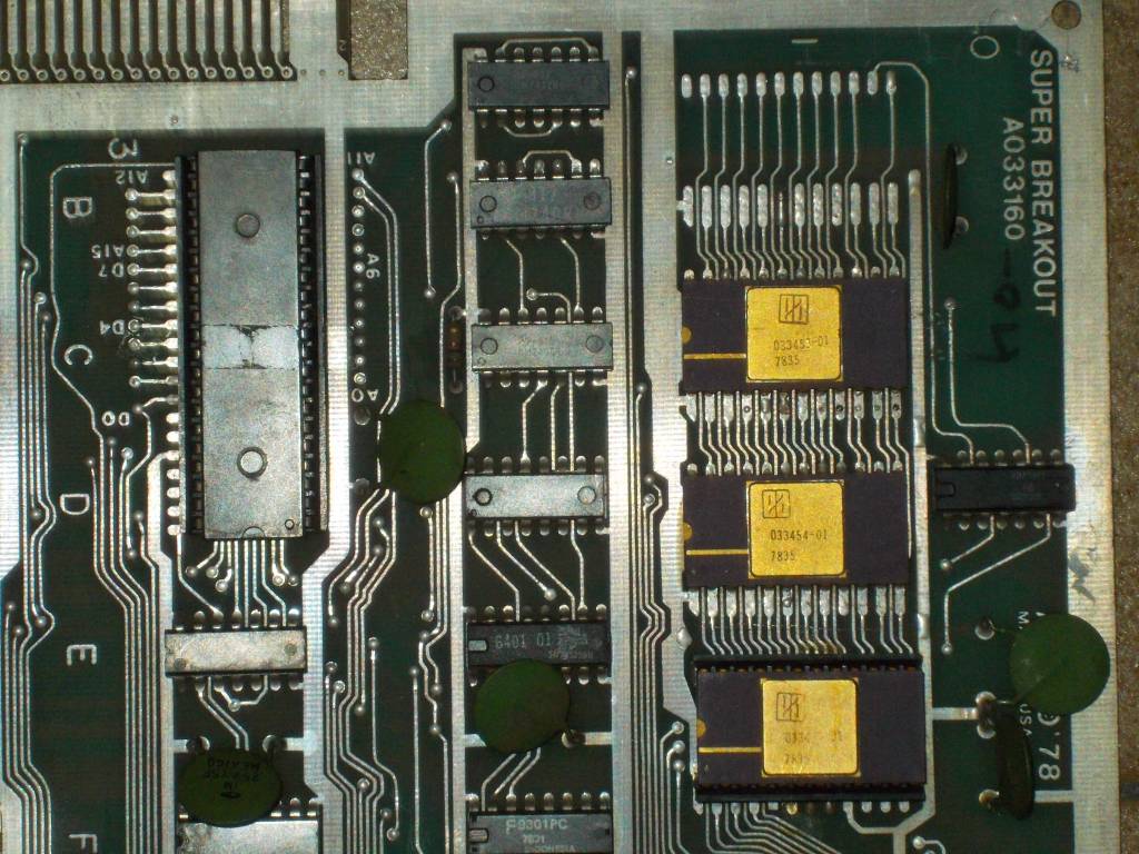
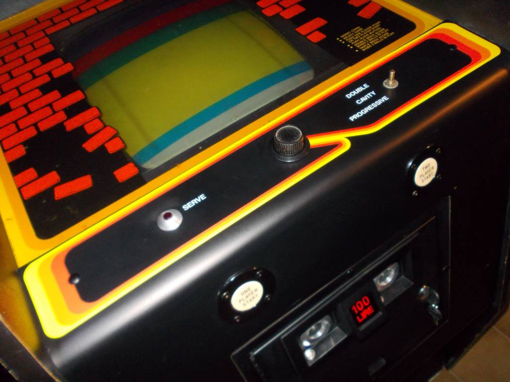
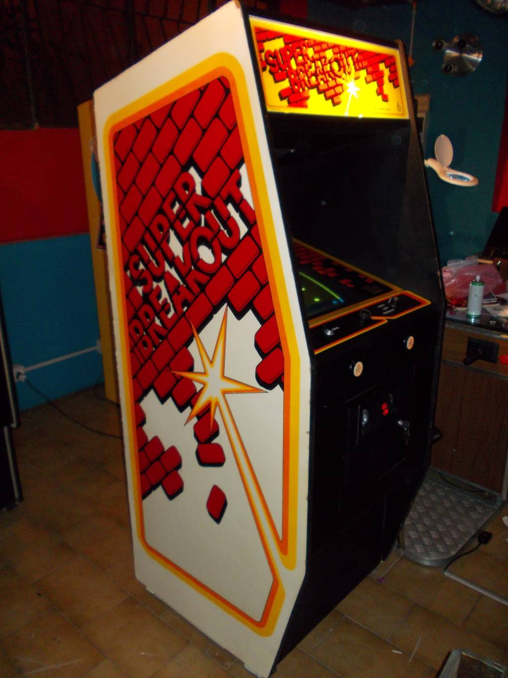
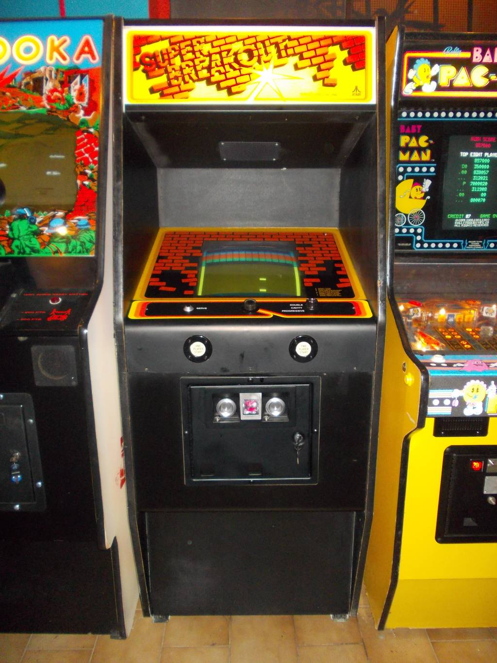
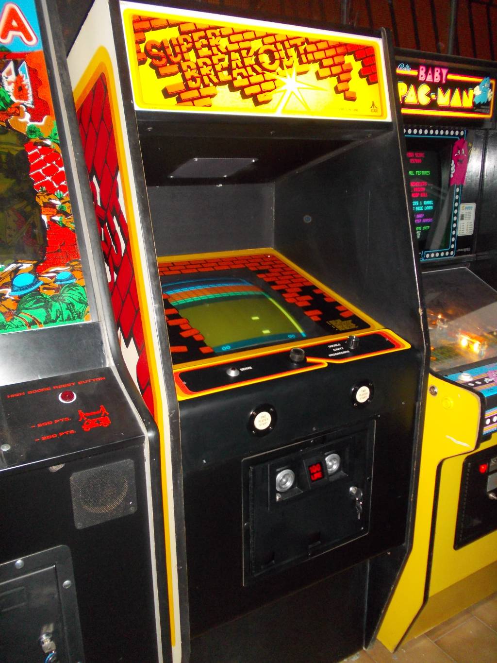
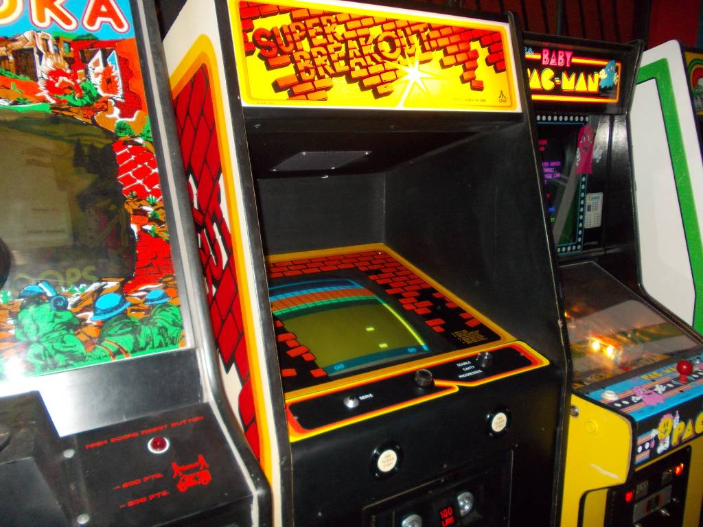
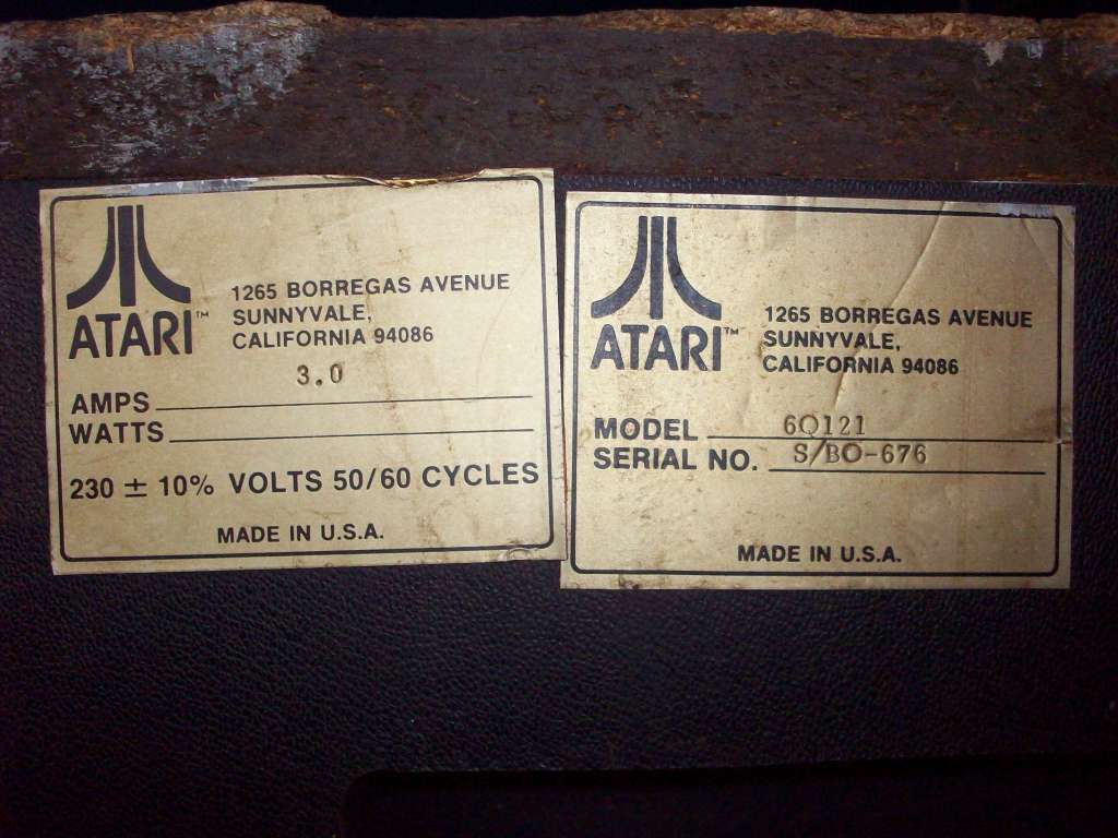
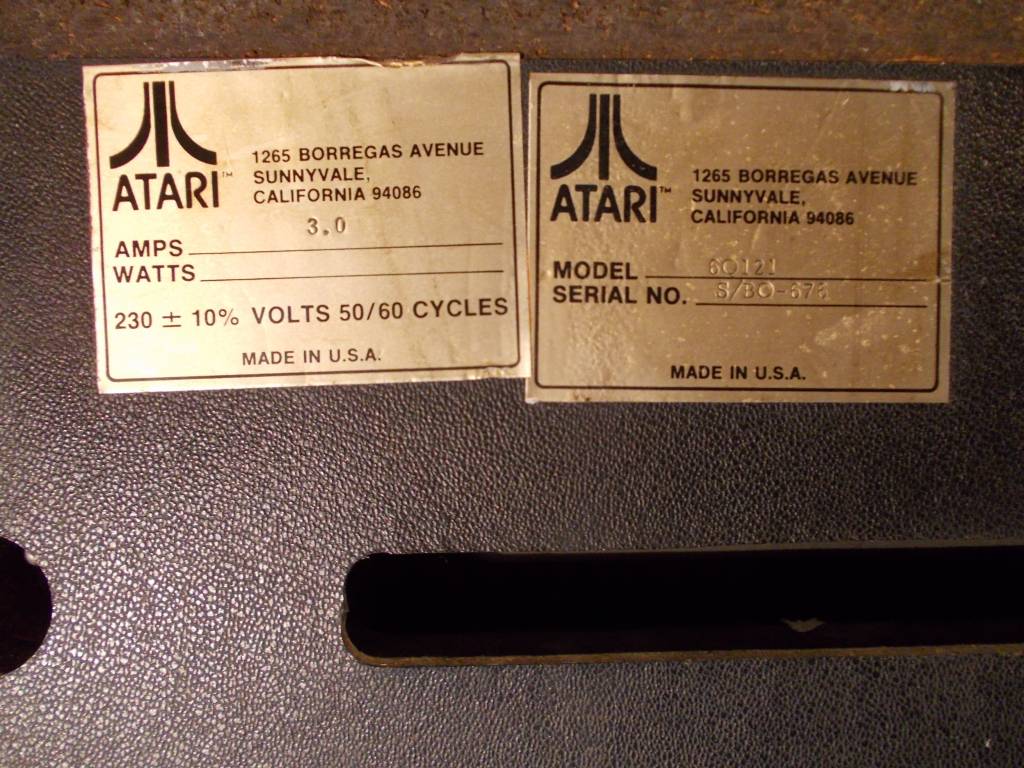
Super Breakout

  • Manufacturer: Atari
  • Year: 1978

Useful info

  • Cabinet type: Upright
  • Measures (WxHxD): 64,5 x 176,8 x 71,0 cm
  • Working voltage: 220V
  • Maximum consumption: 118,0W 0,765A
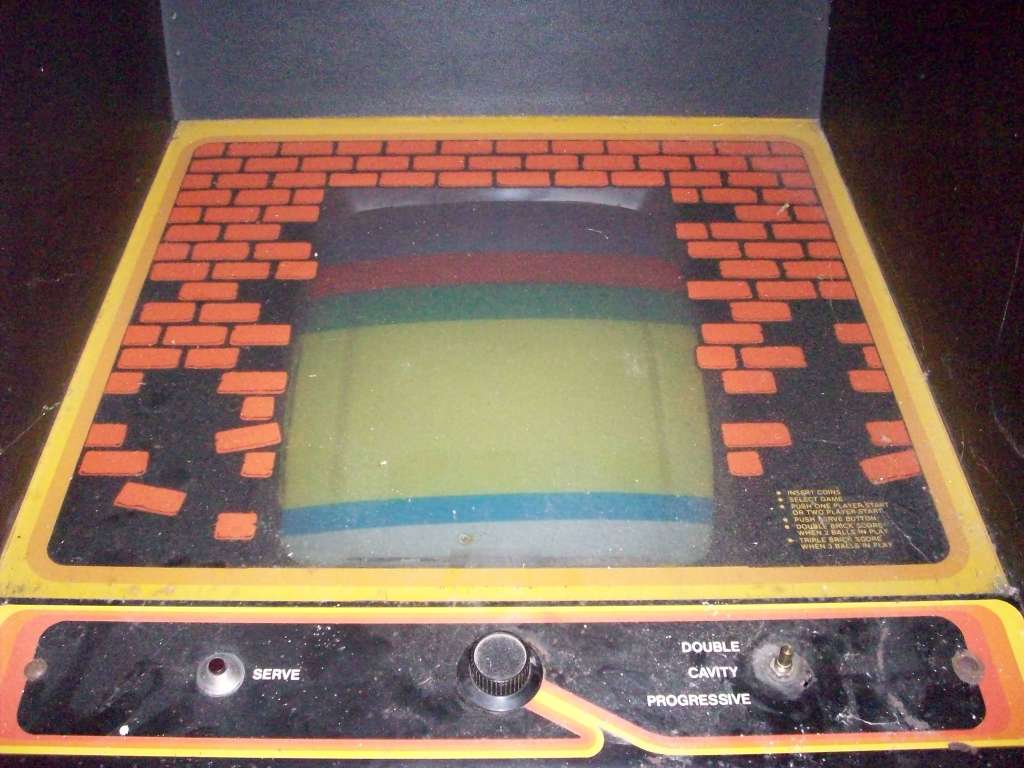
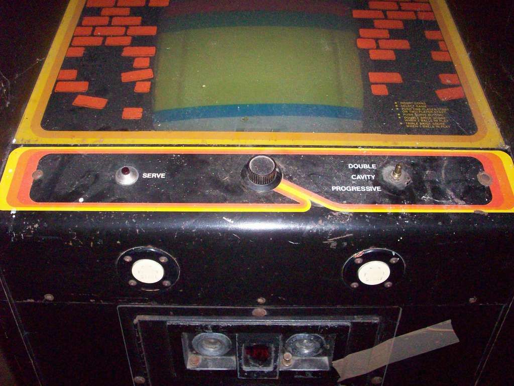
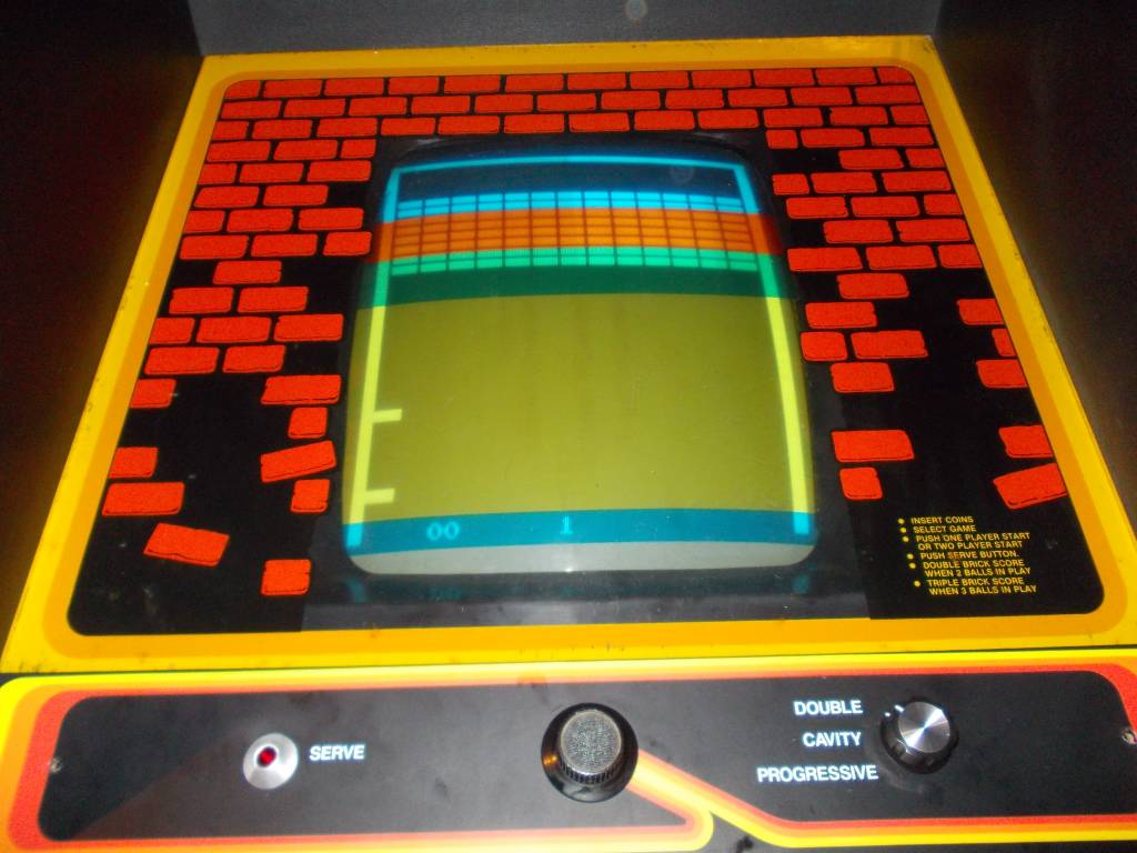
  • Technology: Vertical B/W raster monitor with colored overlay

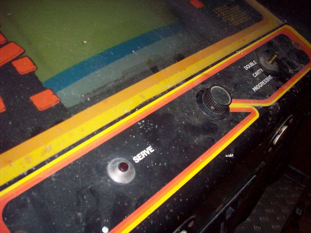
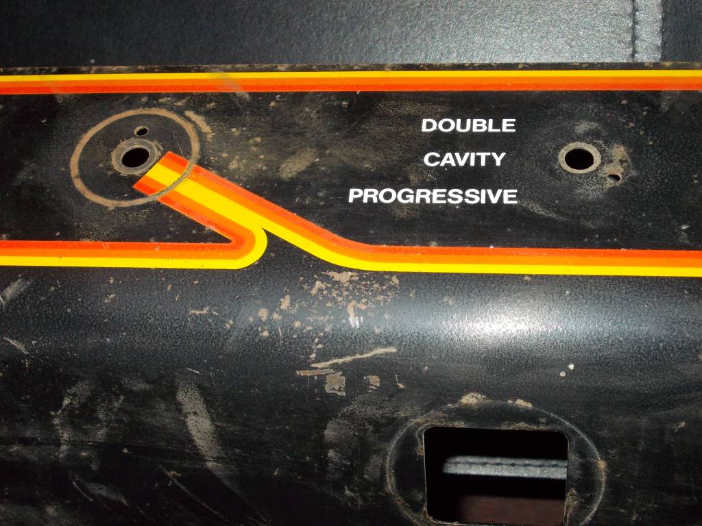
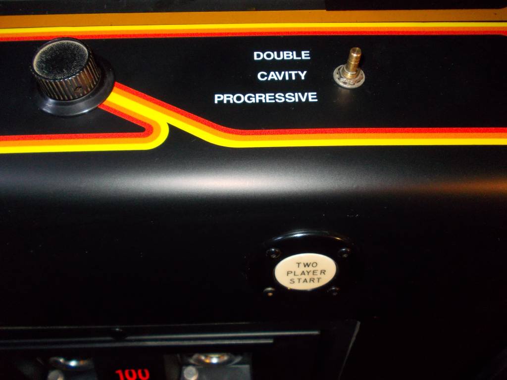
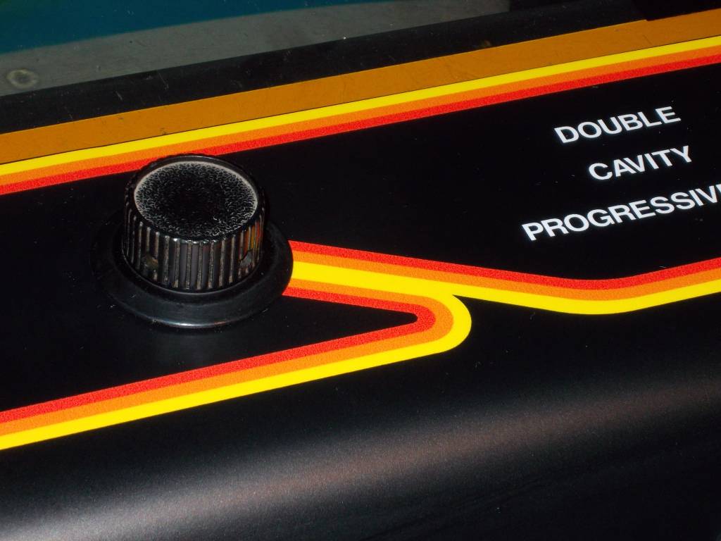
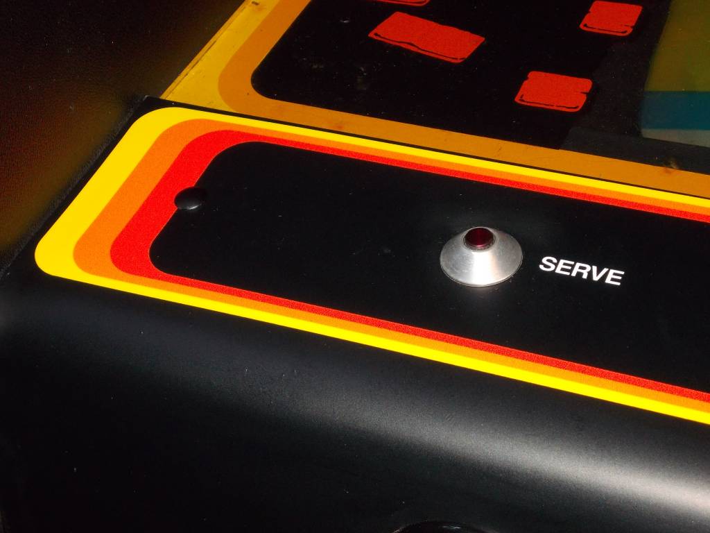
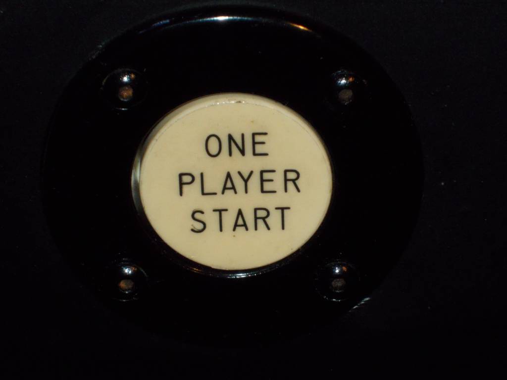
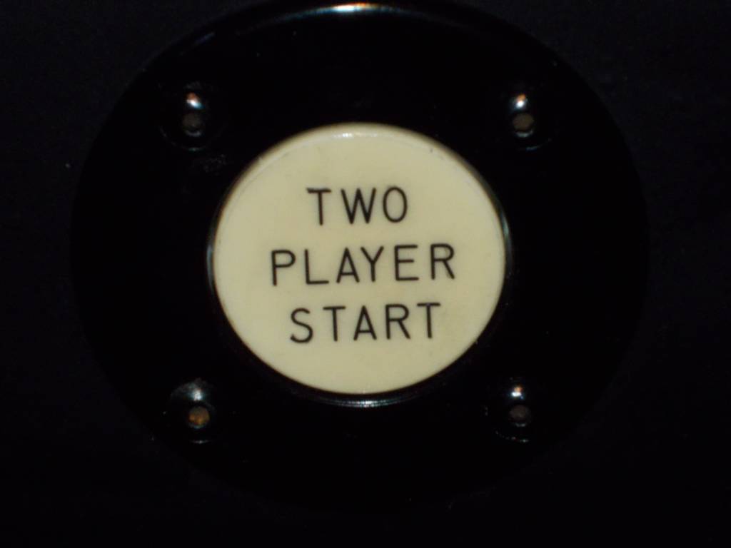
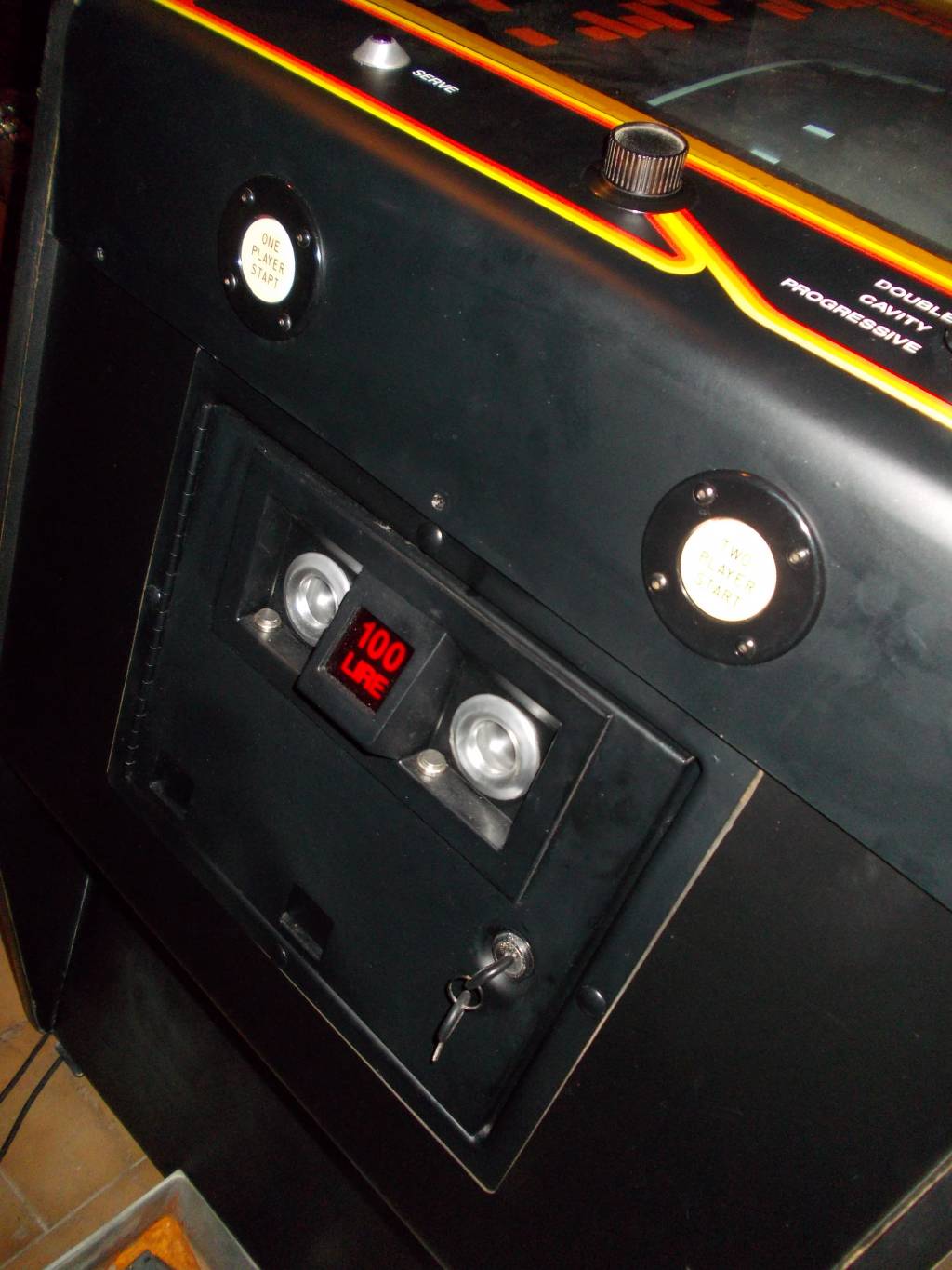
It is the second part of the first and most famous game of the “wall”, Breakout. The player controls a horizontal paddle at the bottom of the screen. A ball bounces off the screen and the player has to prevent it from leaving the only open side. Once taken, the ball bounces on the overlying wall, destroying all the bricks it meets. As the game progresses, the ball’s speed up. This evolution (“Super” not for nothing) gives the player the possibility to choose 3 game modes by turning a knob before the game starts. The game modes are as follows:

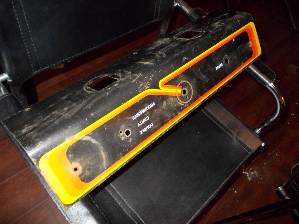
  • Double: two paddles lined up with two balls simultaneously.
  • Cavity: two balls are trapped inside the wall; once released, they can be used to continue the game.
  • Prog: as the game progresses the wall moves down approaching the paddle making the play field more narrow and cramped.

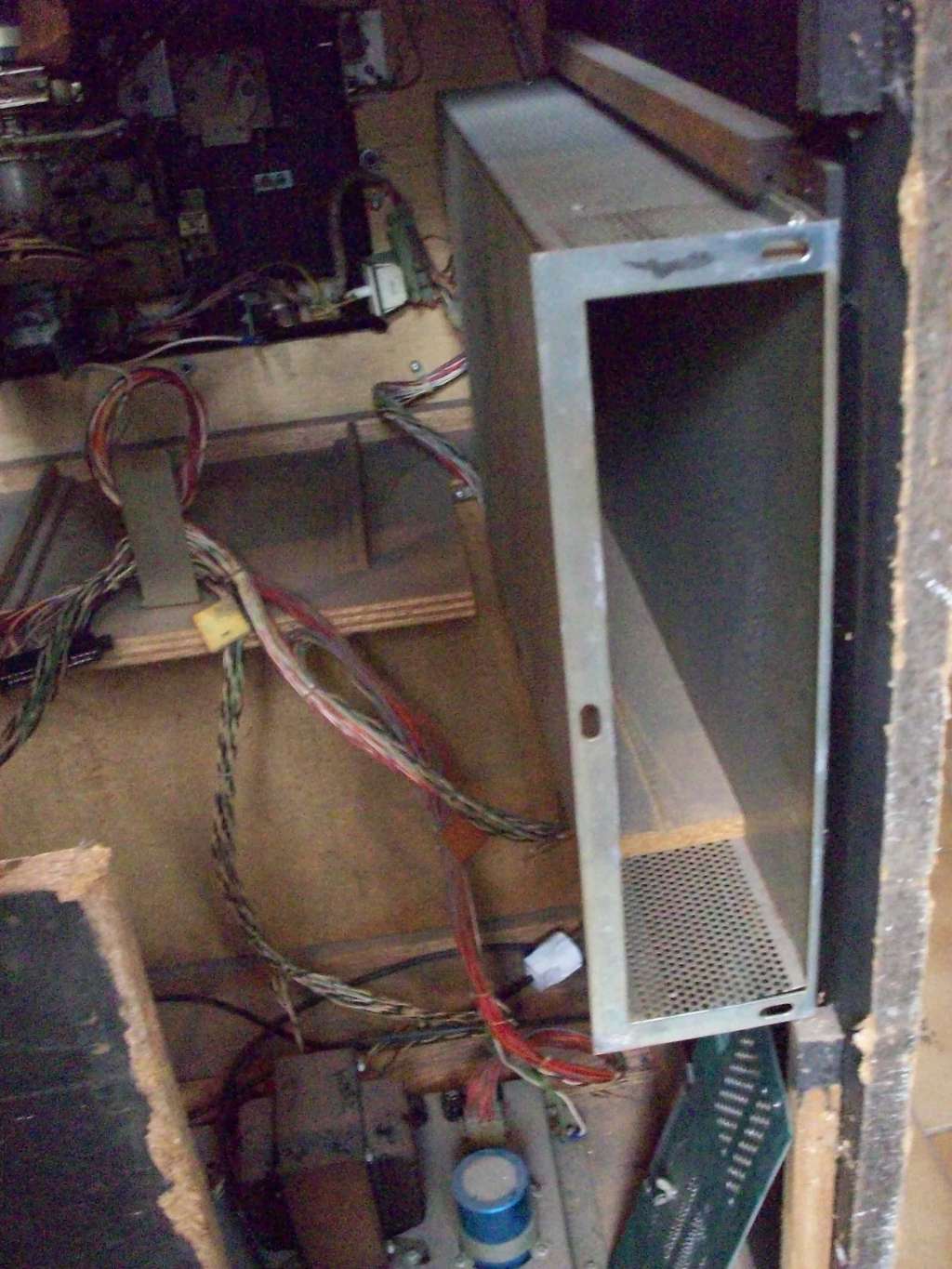
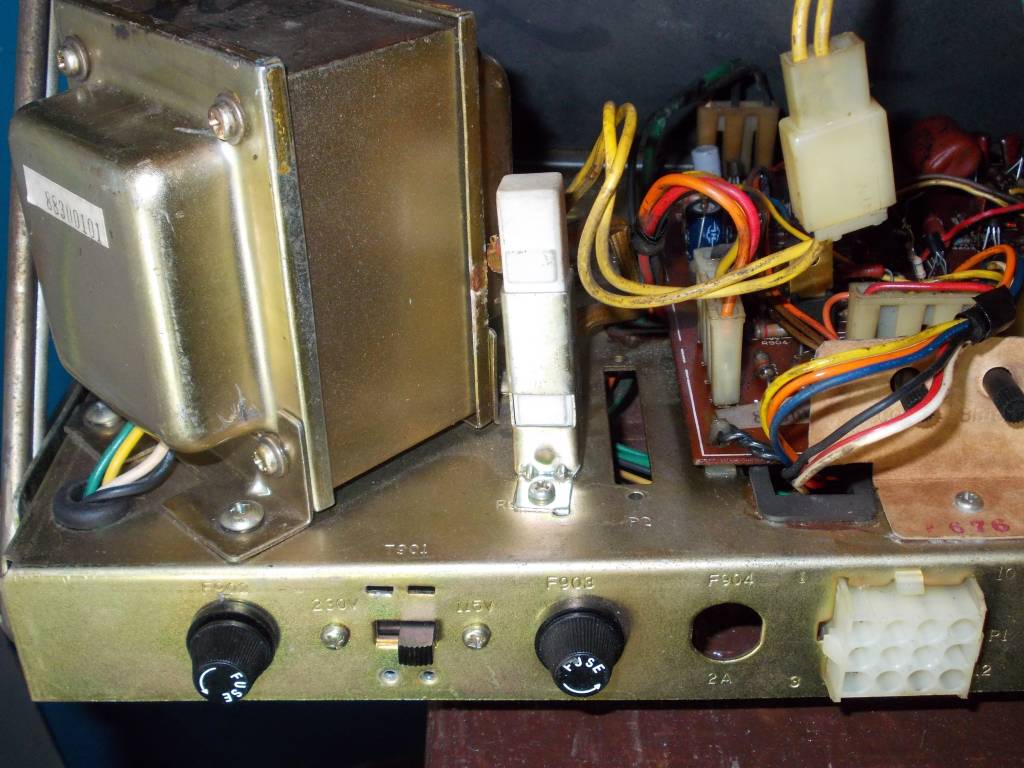
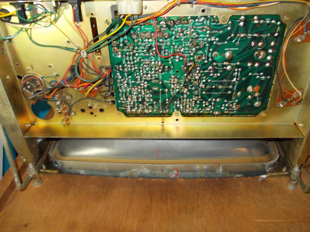
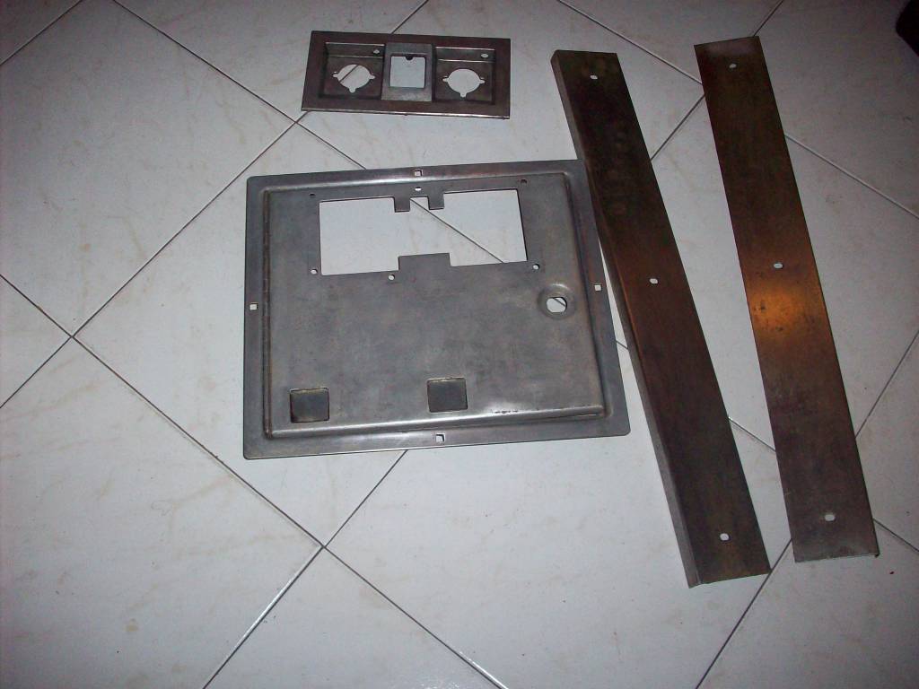
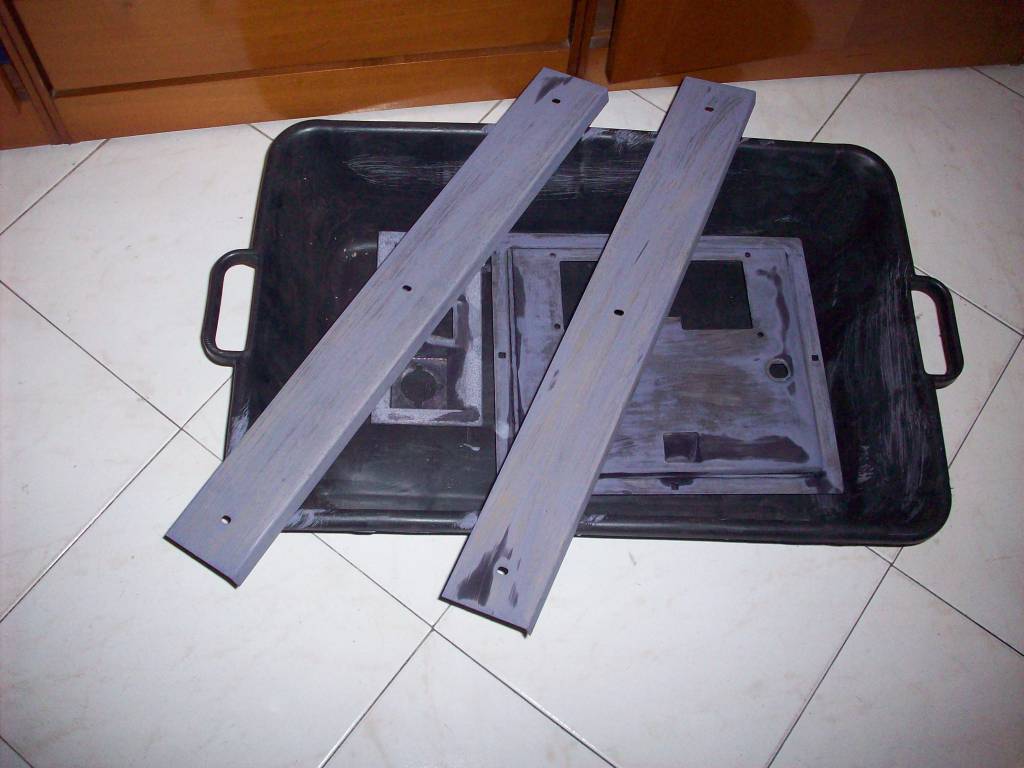
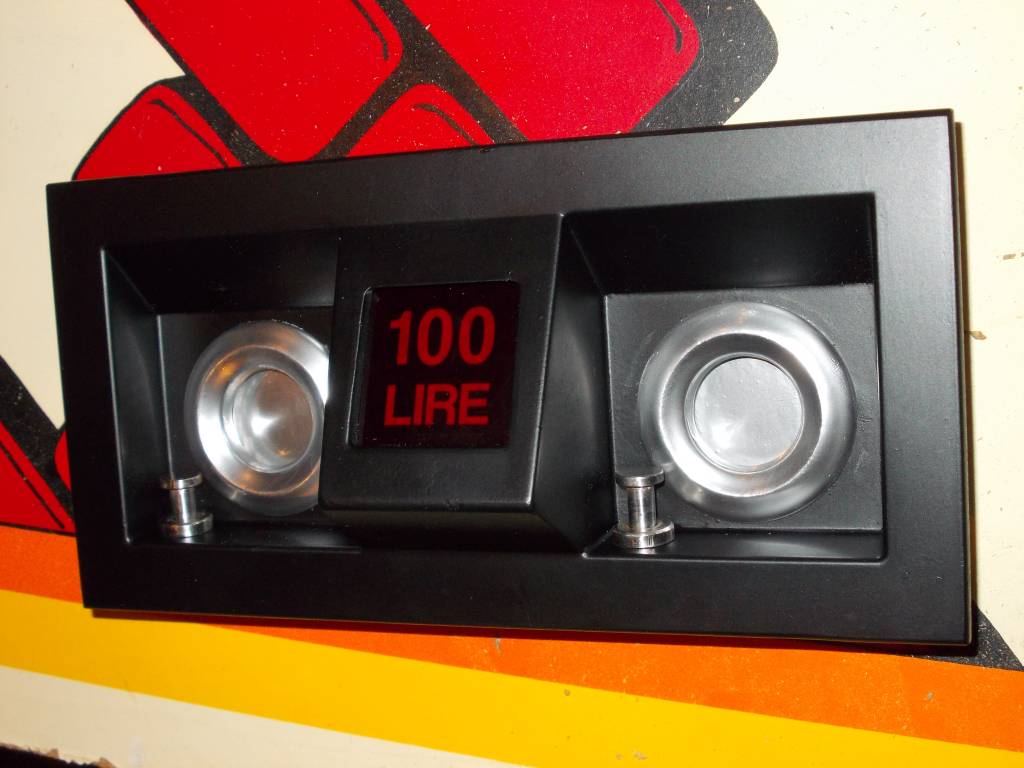
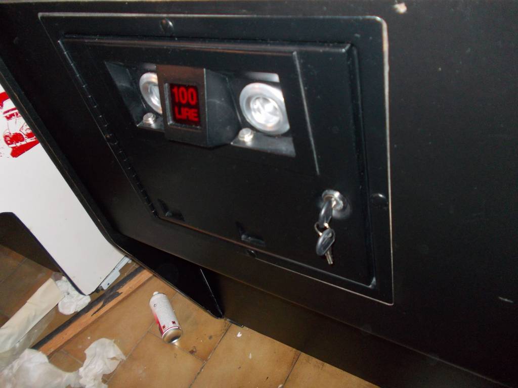
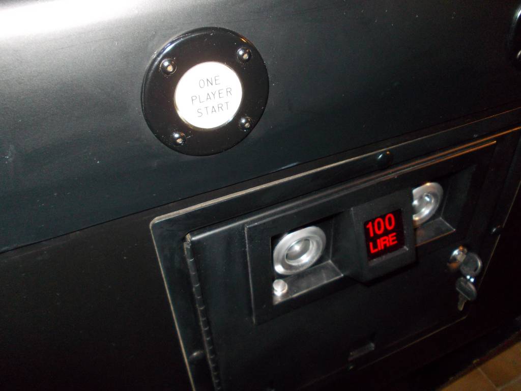
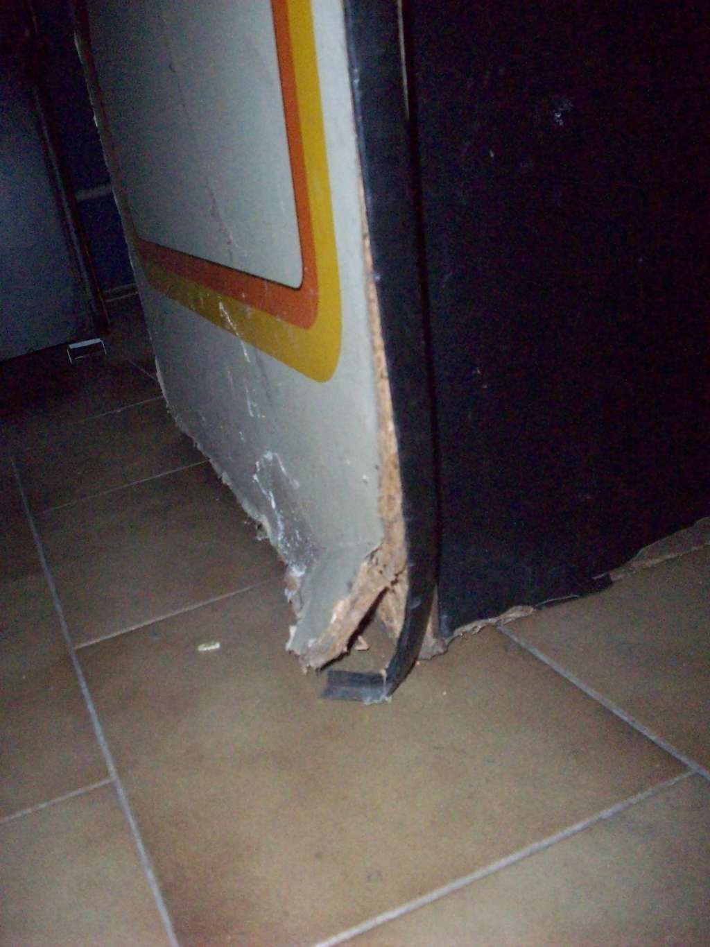
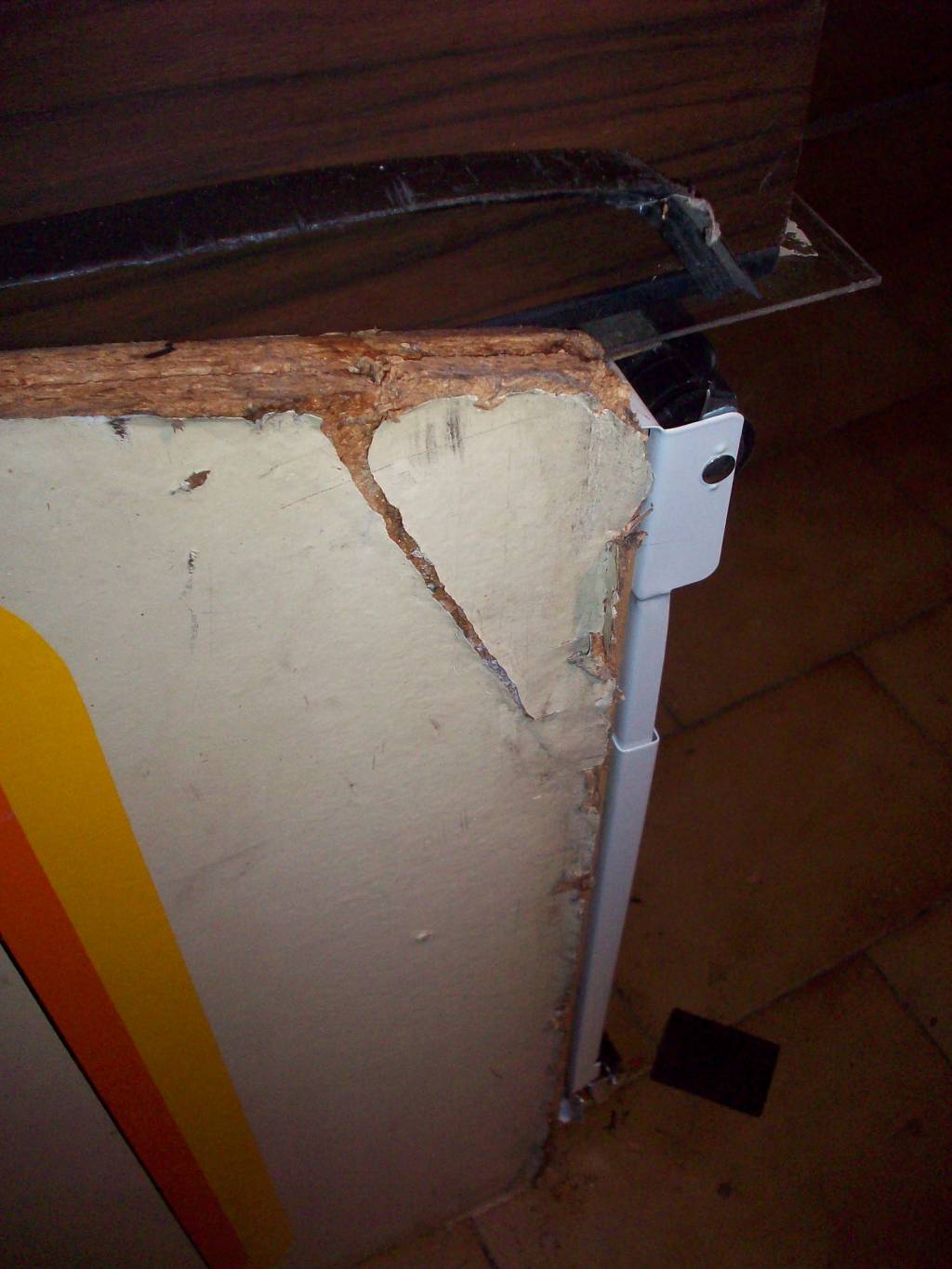
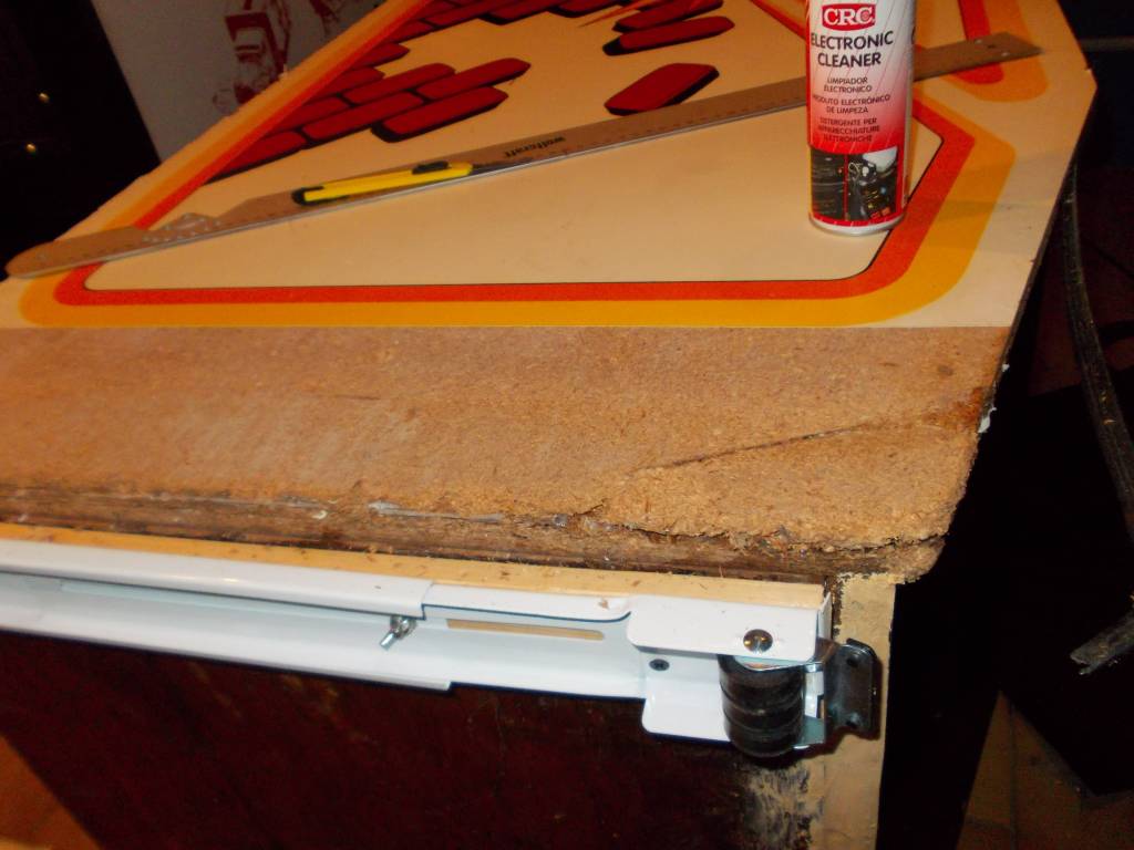
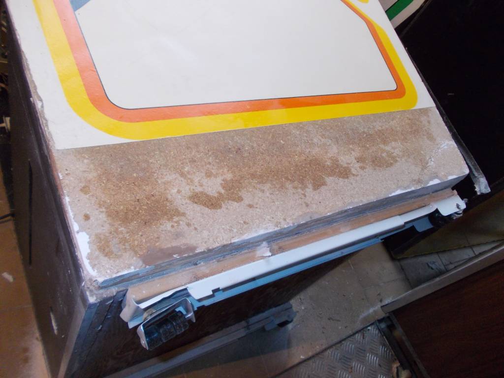
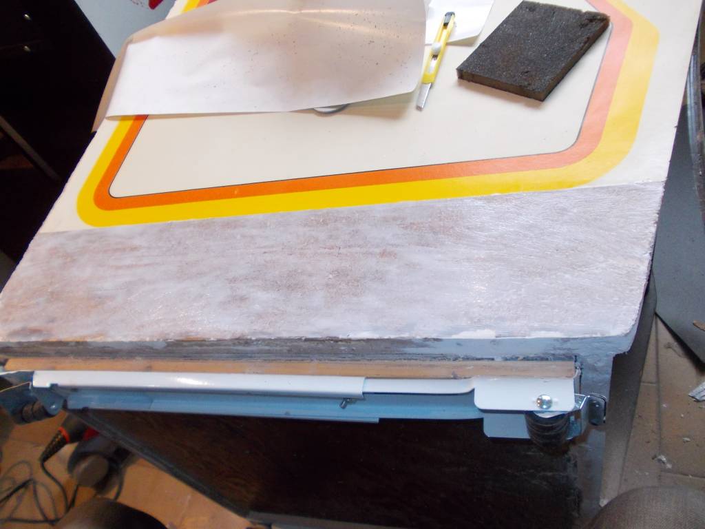
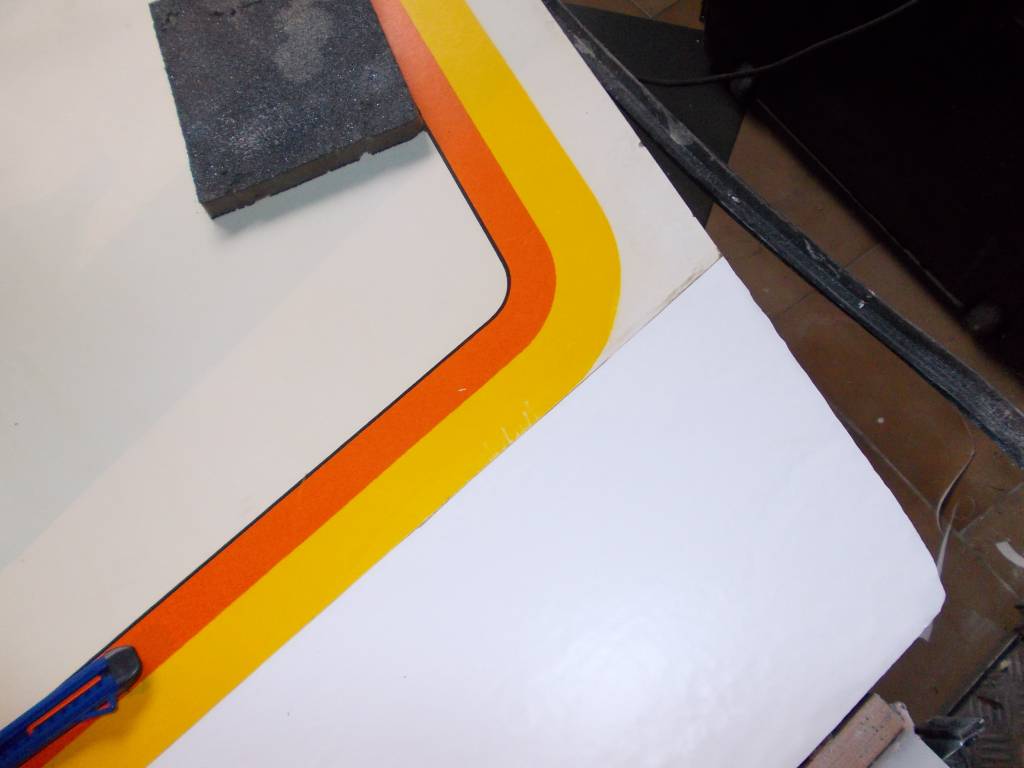
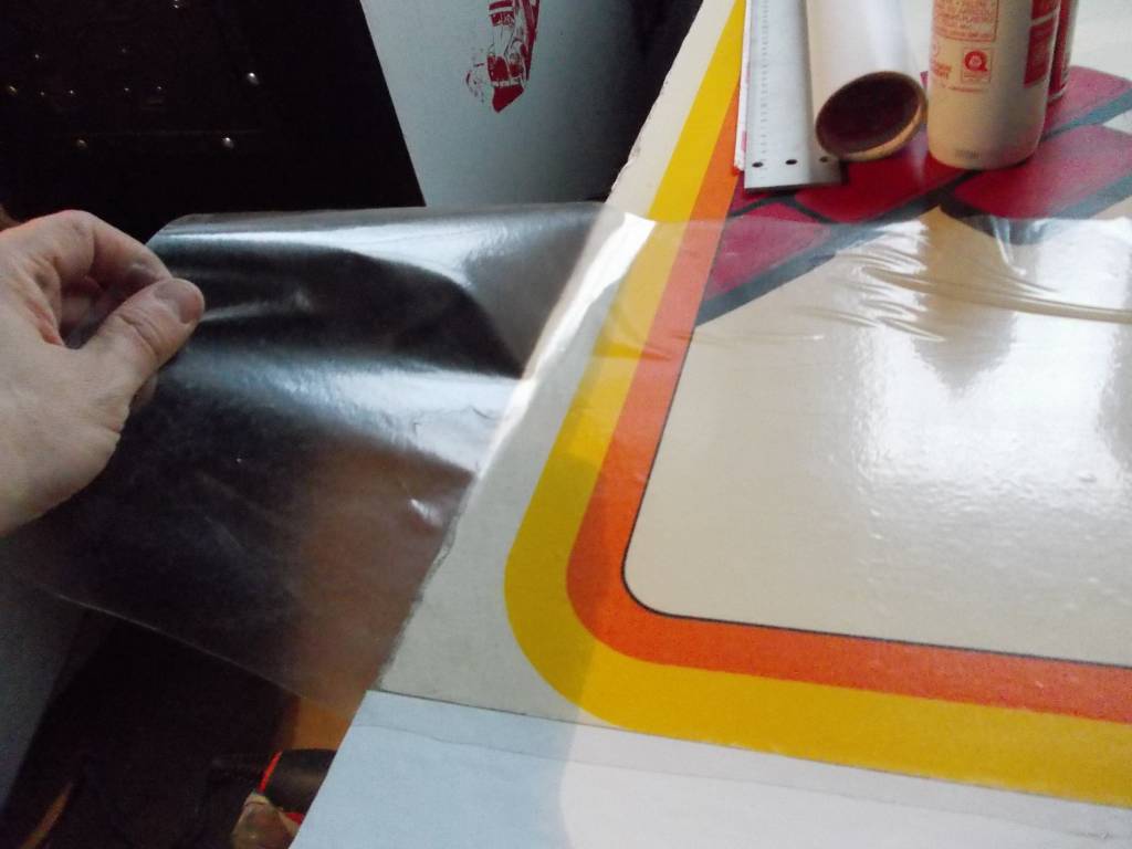
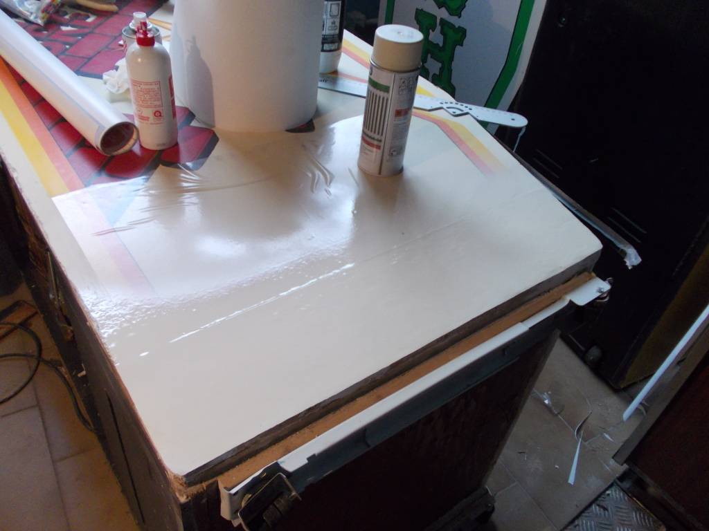
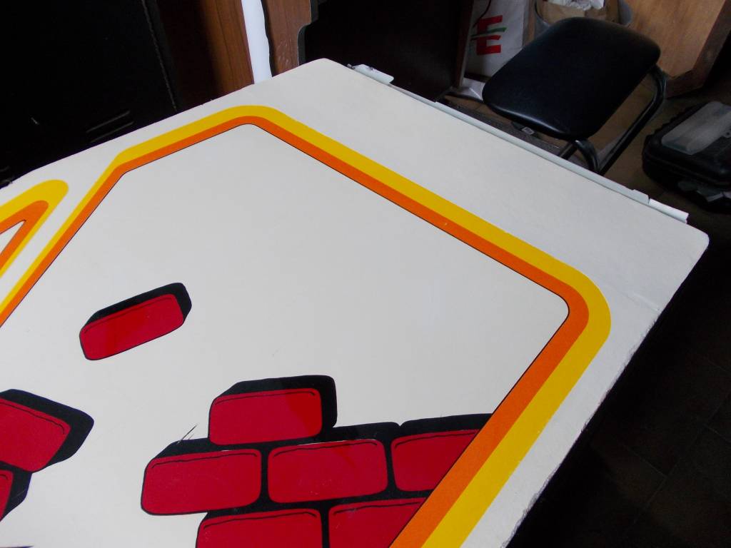
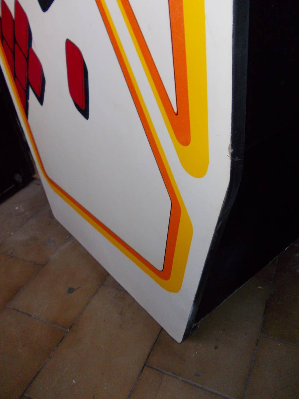
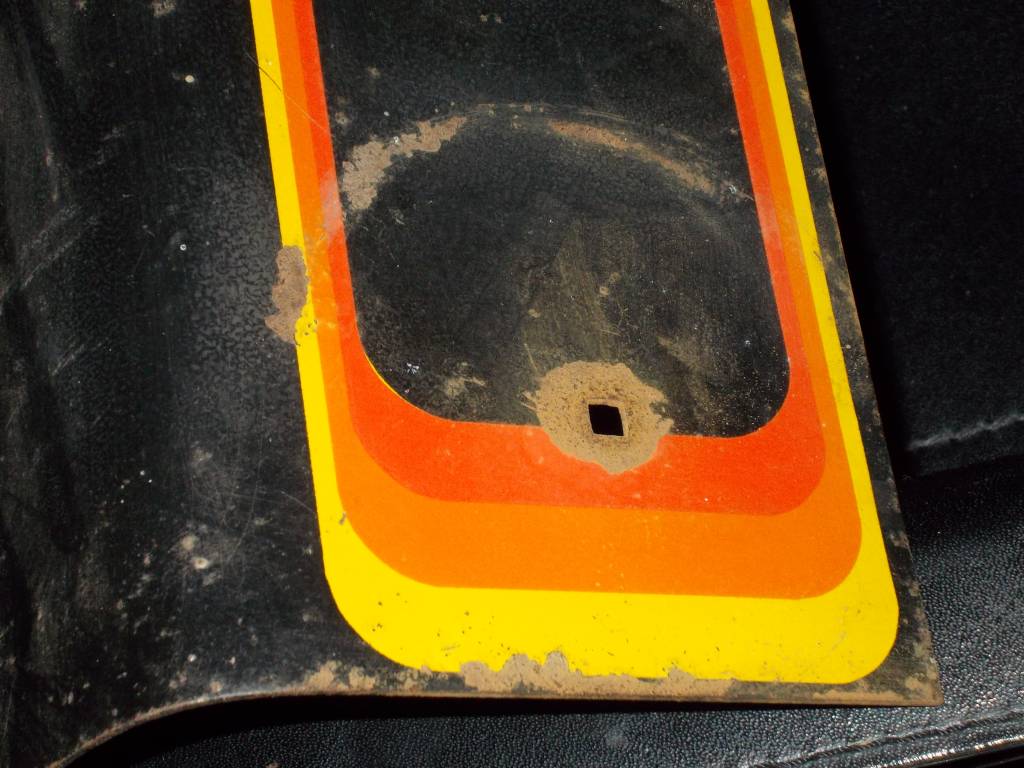
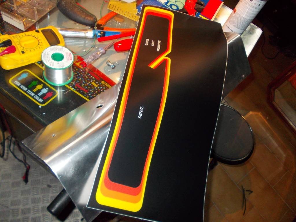
This cabinet  is completely original in the US version and in excellent aesthetic condition. The plexiglass have been regenerated and the side art partially reconstructed where needed.

Three games, one cab!

8 April 2014

I think Super Breakout is very cool. I’ve been lucky to find it… in Germany of course…

100_0670 100_0681 100_0676 100_0678 100_0685 100_0689


Inside

8 April 2014

First of all I removed everything from inside. Cleaned. And remounted.

100_0676 100_0677 100_0688 100_0690 100_0691 100_0692 Dscn0546 Dscn0556 Dscn0557 Dscn0579


PCB

8 April 2014

The PCB was in quite good conditions.


Dscn0525
Dscn0537 Dscn0540 Dscn0541 Dscn0542 Dscn0544 Dscn0545

TV

9 April 2014

This is the TV inside the cab. I needed a lot of time to put it in working conditions. I had no HV at all and I troubleshooted all H circuit without any  result. After a lot of time I found a soldering that had not contact with the components.

Dscn0517 Dscn0518 Dscn0519 Dscn0520 Dscn0521 Dscn0522

Front

9 April 2014

The front panel was damaged and I decided to remake it.

superbreakout_front01

superbreakout_front02 superbreakout_front03 superbreakout_front04 superbreakout_front07

Coin door

9 April 2014

Usual job for the coin door…

superbreakout_coindoor_01 superbreakout_coindoor_02 superbreakout_coindoor_03 superbreakout_coindoor_04 superbreakout_coindoor_05 superbreakout_coindoor_06 superbreakout_coindoor_07 superbreakout_coindoor_08 superbreakout_coindoor_09 superbreakout_coindoor_10 superbreakout_coindoor_11 superbreakout_coindoor_12 superbreakout_coindoor_14 superbreakout_coindoor_15

Left side

9 April 2014

Left side was damaged. Probably I did it during the transport.

  1. I prepared the smooth surface
  2. I used an adhesive white vinyl
  3. I covered the colored parts
  4. I used ivory spray paint in order to have no differences between the old white side art and the new “patch”

 Phase 1

100_0683 100_0701 100_0718 Dscn0041 Dscn0059 Dscn0061


Phase 2

Dscn0065


Phase 3

Dscn0067


Phase 4

Dscn0069

This is the result.

Dscn0117 Dscn0124


CP overlay

9 April 2014

CP needed to be restored. I didn’t want to destroy the original I had so I proceeded in the following way:

  • I removed all parts from the control panel
  • I cleaned the surface
  • I put an aluminium sheet covering all the control panel
  • then I printed on vinyl the CP overlay
  • I used this adhesive overlay on the aluminium

100_0680

100_0697 Dscn0269 Dscn0270 Dscn0271 Dscn0273 Dscn0275 Dscn0277 Dscn0290 Dscn0292 Dscn0293 Dscn0303 Dscn0304


I covered with a transparent overlay both start buttons

Dscn0305 Dscn0306 Dscn0307

The end

9 April 2014

This is the final result of the work

Dscn0574 Dscn0576 Dscn0577 Dscn0581 Dscn0583 Dscn0584 Dscn0586 Dscn0587

PCB troubleshooting

9 April 2014

One day, after some hours of playing, board became faulty. Test gave an error on BIT 7 Following the schematics I checked all components involved in the management of this bit and all components more or less related but nothing happened. This is the part of the schematics I used.

Image2

After some other checks I found the faulty IC: 9322 (=74157) in J2. In practice  A7 wasn’t managed correctly.